Special Function Registers :
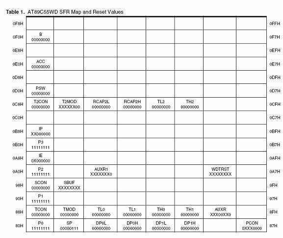
A map of the on-chip memory area called the Special Function Register (SFR) space is shown
in Table 1.
Note that not all of the addresses are occupied, and unoccupied addresses may not be implemented
on the chip. Read accesses to these addresses will in general return random data,
and write accesses will have an indeterminate effect.
User software should not write 1s to these unlisted locations, since they may be used in future
products to invoke new features. In that case, the reset or inactive values of the new bits will
always be 0.
Timer 2 Registers: Control and status bits are contained in registers T2CON (shown in Table
2) and T2MOD (shown in Table 2) for Timer 2. The register pair (RCAP2H, RCAP2L) are the
Capture/Reload registers for Timer 2 in 16-bit capture mode or 16-bit auto-reload mode.
AVR Atmega 128 Features :

• High-performance, Low-power AVR® 8-bit Microcontroller
• Advanced RISC Architecture
– 133 Powerful Instructions – Most Single Clock Cycle Execution
– 32 x 8 General Purpose Working Registers + Peripheral Control Registers
– Fully Static Operation
– Up to 16 MIPS Throughput at 16 MHz
– On-chip 2-cycle Multiplier
• Nonvolatile Program and Data Memories
– 128K Bytes of In-System Reprogrammable Flash
Endurance: 10,000 Write/Erase Cycles
– Optional Boot Code Section with Independent Lock Bits
In-System Programming by On-chip Boot Program
True Read-While-Write Operation
– 4K Bytes EEPROM
Endurance: 100,000 Write/Erase Cycles
– 4K Bytes Internal SRAM
– Up to 64K Bytes Optional External Memory Space
– Programming Lock for Software Security
– SPI Interface for In-System Programming
• JTAG (IEEE std. 1149.1 Compliant) Interface
– Boundary-scan Capabilities According to the JTAG Standard
– Extensive On-chip Debug Support
– Programming of Flash, EEPROM, Fuses and Lock Bits through the JTAG Interface
• Peripheral Features
– Two 8-bit Timer/Counters with Separate Prescalers and Compare Modes
– Two Expanded 16-bit Timer/Counters with Separate Prescaler, Compare Mode and
Capture Mode
– Real Time Counter with Separate Oscillator
– Two 8-bit PWM Channels
– 6 PWM Channels with Programmable Resolution from 2 to 16 Bits
– Output Compare Modulator
– 8-channel, 10-bit ADC
8 Single-ended Channels
7 Differential Channels
2 Differential Channels with Programmable Gain at 1x, 10x, or 200x
– Byte-oriented Two-wire Serial Interface
– Dual Programmable Serial USARTs
– Master/Slave SPI Serial Interface
– Programmable Watchdog Timer with On-chip Oscillator
– On-chip Analog Comparator
• Special Microcontroller Features
– Power-on Reset and Programmable Brown-out Detection
– Internal Calibrated RC Oscillator
– External and Internal Interrupt Sources
– Six Sleep Modes: Idle, ADC Noise Reduction, Power-save, Power-down, Standby,
and Extended Standby
– Software Selectable Clock Frequency
– ATmega103 Compatibility Mode Selected by a Fuse
– Global Pull-up Disable
• I/O and Packages
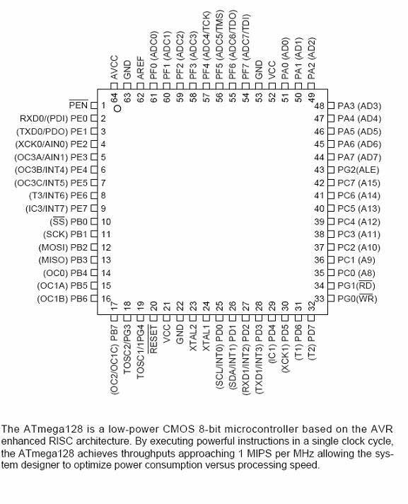
– 53 Programmable I/O Lines
– 64-lead TQFP and 64-pad MLF
• Operating Voltages
– 2.7 - 5.5V for ATmega128L
– 4.5 - 5.5V for ATmega128
• Speed Grades
– 0 - 8 MHz for ATmega128L
– 0 - 16 MHz for ATmega128
Configurations :
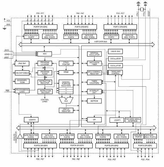
Block Diagram:
ATmega103 and ATmega128 Compatibility :
The AVR core combines a rich instruction set with 32 general purpose working registers.
All the 32 registers are directly connected to the Arithmetic Logic Unit (ALU), allowing
two independent registers to be accessed in one single instruction executed in one clock
cycle. The resulting architecture is more code efficient while achieving throughputs up to
ten times faster than conventional CISC microcontrollers.
The ATmega128 provides the following features: 128K bytes of In-System Programmable
Flash with Read-While-Write capabilities, 4K bytes EEPROM, 4K bytes SRAM, 53
general purpose I/O lines, 32 general purpose working registers, Real Time Counter
(RTC), four flexible Timer/Counters with compare modes and PWM, 2 USARTs, a byte
oriented Two-wire Serial Interface, an 8-channel, 10-bit ADC with optional differential
input stage with programmable gain, programmable Watchdog Timer with Internal Oscillator,
an SPI serial port, IEEE std. 1149.1 compliant JTAG test interface, also used for
accessing the On-chip Debug system and programming and six software selectable
power saving modes. The Idle mode stops the CPU while allowing the SRAM,
Timer/Counters, SPI port, and interrupt system to continue functioning. The Powerdown
mode saves the register contents but freezes the Oscillator, disabling all other
chip functions until the next interrupt or Hardware Reset. In Power-save mode, the asynchronous
timer continues to run, allowing the user to maintain a timer base while the
rest of the device is sleeping. The ADC Noise Reduction mode stops the CPU and all
I/O modules except Asynchronous Timer and ADC, to minimize switching noise during
ADC conversions. In Standby mode, the Crystal/Resonator Oscillator is running while
the rest of the device is sleeping. This allows very fast start-up combined with low power
consumption. In Extended Standby mode, both the main Oscillator and the Asynchronous
Timer continue to run.
The device is manufactured using Atmel’s high-density nonvolatile memory technology.
The On-chip ISP Flash allows the program memory to be reprogrammed in-system
through an SPI serial interface, by a conventional nonvolatile memory programmer, or
by an On-chip Boot program running on the AVR core. The boot program can use any
interface to download the application program in the application Flash memory. Software
in the Boot Flash section will continue to run while the Application Flash section is
updated, providing true Read-While-Write operation. By combining an 8-bit RISC CPU
with In-System Self-Programmable Flash on a monolithic chip, the Atmel ATmega128 is
a powerful microcontroller that provides a highly flexible and cost effective solution to
many embedded control applications.
The ATmega128 AVR is supported with a full suite of program and system development
tools including: C compilers, macro assemblers, program debugger/simulators, in-circuit
emulators, and evaluation kits.
The ATmega128 is a highly complex microcontroller where the number of I/O locations
supersedes the 64 I/O locations reserved in the AVR instruction set. To ensure backward
compatibility with the ATmega103, all I/O locations present in ATmega103 have
the same location in ATmega128. Most additional I/O locations are added in an
Extended I/O space starting from $60 to $FF, (i.e., in the ATmega103 internal RAM
space). These locations can be reached by using LD/LDS/LDD and ST/STS/STD
instructions only, not by using IN and OUT instructions. The relocation of the internal
RAM space may still be a problem for ATmega103 users. Also, the increased number of
interrupt vectors might be a problem if the code uses absolute addresses. To solve
these problems, an ATmega103 compatibility mode can be selected by programming
the fuse M103C. In this mode, none of the functions in the Extended I/O space are in
use, so the internal RAM is located as in ATmega103. Also, the Extended Interrupt vectors
are removed.
ATmega103 Compatibility Mode :
The ATmega128 is 100% pin compatible with ATmega103, and can replace the
ATmega103 on current Printed Circuit Boards. The application note “Replacing
ATmega103 by ATmega128” describes what the user should be aware of replacing the
ATmega103 by an ATmega128.
By programming the M103C fuse, the ATmega128 will be compatible with the
ATmega103 regards to RAM, I/O pins and interrupt vectors as described above. However,
some new features in ATmega128 are not available in this compatibility mode,
these features are listed below:
• One USART instead of two, Asynchronous mode only. Only the eight least
significant bits of the Baud Rate Register is available.
• One 16 bits Timer/Counter with two compare registers instead of two 16-bit
Timer/Counters with three compare registers.
• Two-wire serial interface is not supported.
• Port C is output only.
• Port G serves alternate functions only (not a general I/O port).
• Port F serves as digital input only in addition to analog input to the ADC.
• Boot Loader capabilities is not supported.
• It is not possible to adjust the frequency of the internal calibrated RC Oscillator.
• The External Memory Interface can not release any Address pins for general I/O,
neither configure different wait-states to different External Memory Address
sections.
In addition, there are some other minor differences to make it more compatible to
ATmega103:
• Only EXTRF and PORF exists in MCUCSR.
• Timed sequence not required for Watchdog Time-out change.
• External Interrupt pins 3 - 0 serve as level interrupt only.
• USART has no FIFO buffer, so data overrun comes earlier.
Unused I/O bits in ATmega103 should be written to 0 to ensure same operation in
ATmega128.
علیرضا عظیمی a.azimi@nceimc.com -
<لیفتیران>


 محل تبلیغ شما
 بیمه آسانسور- بیمه ما
 آموزشگاه آسانسور آرمان فراز پیمان
 آسانور-تولید کننده تابلو فرمان آسانسور
 محل تبلیغ شما
 تله کابین77539630

 موسسه خیریه محک
 آسانسور 110 - نماینده فروش قطعات آسانسور هیدرولیک ویتور
 محاسبه و نقشه کشی خودکار آسانسور
 محل درج آگهی شما
 شرکت بازرسی و مهندسی ایران
 مجله دنیای آسانسور
 امور حسابداری-حسابرسی-بیمه
 بیمه آسانسور: البرز
 خدمات محاسبه، طراحی و تهیه نقشه آسانسور